


pcb production and assembly suitable for high-speed applications
In the relentless pursuit of faster and more efficient electronic devices, the suitability of Printed Circuit Board (PCB) production and assembly for high-speed applications becomes a critical consideration. High-speed applications, characterized by the need for rapid data transmission, low signal loss, and minimal electromagnetic interference (EMI), pose unique challenges that demand specialized design, manufacturing, and assembly techniques to ensure optimal performance.
At the heart of high-speed PCB design lies meticulous attention to signal integrity. Signal traces must be carefully routed to minimize impedance mismatches, signal reflections, and crosstalk, which can degrade signal quality and impair system performance. Advanced design software, coupled with experienced engineers, enables the optimization of trace geometries, layer stackups, and grounding strategies to mitigate signal integrity issues and maximize data throughput.
The production of pcb production and assembly suitable for high-speed applications involves precision manufacturing processes that adhere to strict tolerances and quality standards. High-frequency laminates, such as Rogers or Teflon-based substrates, offer superior dielectric properties and low loss tangents, minimizing signal attenuation and distortion at GHz frequencies. Advanced fabrication techniques, including controlled impedance routing, fine-line etching, and laser drilling, ensure the precise replication of design specifications and maintain signal integrity throughout the PCB.
Are pcb production and assembly suitable for high-speed applications?
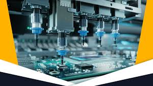
Moreover, the assembly of high-speed PCBs requires careful consideration of component placement, soldering techniques, and interconnection methods to minimize parasitic effects and signal degradation. Surface-mount technology (SMT) components, characterized by their compact size and short lead lengths, are preferred for high-speed applications to reduce parasitic capacitance and inductance. Additionally, controlled soldering processes, such as reflow soldering with optimized thermal profiles, ensure reliable and consistent solder joints that meet the stringent requirements of high-speed signal transmission.
In addition to design and assembly considerations, rigorous testing and validation are essential to verify the performance of high-speed PCBs. Signal integrity analysis, including time-domain reflectometry (TDR) and eye diagram analysis, enables engineers to characterize signal quality, identify potential issues, and optimize PCB designs accordingly. Compliance testing for electromagnetic compatibility (EMC) ensures that high-speed PCBs meet regulatory standards and exhibit minimal susceptibility to EMI from external sources.
Despite the inherent challenges, PCB production and assembly have proven to be highly suitable for high-speed applications across a diverse range of industries. From telecommunications and data networking to aerospace and automotive systems, high-speed PCBs enable the rapid and reliable transmission of critical data, supporting the advancement of technology and innovation.
Furthermore, advancements in materials science, manufacturing techniques, and assembly technologies continue to push the boundaries of what is achievable in high-speed PCB design. Emerging technologies, such as embedded capacitance and advanced interconnect solutions, offer novel approaches to further enhance signal integrity and reduce transmission losses in high-speed PCBs.
In conclusion, PCB production and assembly are well-suited for high-speed applications, provided that meticulous attention is paid to design considerations, manufacturing processes, and testing methodologies. By leveraging advanced design tools, materials, and techniques, engineers can develop high-speed PCBs that meet the stringent performance requirements of today’s demanding applications. As technology continues to evolve, the capabilities of PCB production and assembly will continue to advance, enabling even faster and more efficient electronic systems in the years to come.