


Pcba printed circuit board
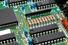
A PCB is the heart of any electronic device. It can be used for a variety of purposes such as powering an LED light or providing a base for a smartphone. However, a PCB is only fully functional after the components are soldered onto it. There are two main types of PCBAs – through-hole and surface-mount. Both are capable of performing different functions, but their assembly methods differ. Whether your project uses through-hole or surface-mount components, there are several ways to make them work together. The most important factors to consider are the type of soldering technique and quality of assembly.
PCBs are typically printed with a legend, which can include identifying text, test points, or components. Historically, this was accomplished with silkscreen printing, but other printing methods can also be used. While these markings are not required for function, they can be useful for referencing the components and locations on the board during assembly and testing.
The first step in a printed circuit board pcba assembly process is applying the solder paste. This is done by placing a stencil over the area of the board where the component will be placed. The stencil is then filled with a sticky solder paste. A pick and place machine then places the component on top of the soldering paste. This is done in accordance with a file created by the designer, which specifies the coordinates of each component on the board.
How are components soldered onto an Pcba printed circuit board?
Once the components have been placed, the next step is to heat them with a hot iron. This step is done in a controlled manner to ensure that the soldering is completed properly and without damage. The heated iron must touch the component and the board, and the iron must remain in contact with both of them for a few seconds. Adding a bit of solder to the iron’s tip can help it better stick to the surface of the component and the board, but this is optional.
After the soldering is complete, the resulting joint must be inspected and tested. This step includes checking for defects such as misaligned components and solder bridges, which can reduce the performance of the finished product. The inspection and testing process may include visual, automated optical, and X-ray inspections, as well as in-circuit and functional tests.
Before starting the soldering process, you must ensure that your work area is clean and free of debris, dust, and grease. Using an industrial cleaning pad is recommended, as it will ensure that the board is free of any contaminants that could cause issues during assembly. In addition, it is best to start with smaller components and then move on to the larger ones. This will help prevent mistakes that can result in cold joints, opened or webbing, lifted pads, solder bridges, and other problems. Using the right tools and following best practices for assembling PCBAs will ensure that your products perform as intended and are of the highest quality.