


Flexible PCBs Accommodate For Dynamic Mechanical Loads
In order to properly design a PCB, the layout must first be created using a Computer Aided Design or CAD system. The most popular software used in the industry is KiCad, which provides a wide range of features and capabilities to help with the design process. Once the design has been finalized and passed the required DRCs, the files must be sent to the manufacturer. Typically, this is done through Gerber files, although other CAD formats can be accepted as well.
Once the PCB is ready for manufacturing, the copper base plating can be applied. Then, a protective solder mask and silk screen can be added to the surface. Finally, components are placed on the board using a pick-and-place machine. This is a machine that has been programmed to read the PCB’s CAD file and place the components according to its specifications. The machine will use a conveyor belt to hold reels or plastic tubes of the various component parts. It then uses a camera to determine the coordinates of the different components. The machine then places these onto the PCB, applying an adhesive to secure them.
While many of the foundational concepts of rigid pcb board are still important to follow when working with a flexible PCB, there are some unique considerations that must be taken into account. For example, the mechanical properties of the material will have a significant impact on how a flexible PCB can be designed to accommodate dynamic mechanical loads.
How Do Flexible PCBs Accommodate For Dynamic Mechanical Loads?
Generally speaking, the thicker a flex PCB’s copper layers are, the more power it can handle. However, these thicker layers can increase the risk of damage when the board is subjected to a dynamic mechanical load. This is because a higher amount of stress will be concentrated on the outermost traces. In order to reduce this stress, it’s important for the flex PCB designer to offset these traces as much as possible.
Another way to reduce stress on a flexible PCB is to choose a larger overall bending radius. This will prevent tensile and compressive stresses from concentrating on the traces on the inner layer at the neutral bending axis. It is also helpful to avoid putting any components on the outside of this arc.
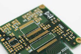
At its core, a PCB is a flat, rigid board made of a non-conductive material, typically fiberglass reinforced with epoxy. This base material, known as the substrate, provides mechanical support and insulation for the circuitry. However, what makes PCBs unique is the thin layer of conductive material laminated onto the substrate, forming a pattern of pathways called traces.
One of the best ways to check if a flex PCB can withstand a dynamic mechanical load is to perform a strain gauge test. This type of test will provide accurate measurements for the strain on the board and give a more precise indication of its strength than FEA tests. These are especially useful for smaller PCBs, as they can’t be inspected with CT scans or X-rays, which can provide limited information about the internal structure of the board.