


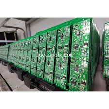
Reliability in PCB Design and Assembly
As a PCB designer, you must ensure your product can stand up to the stresses it will face in its application environment. To do this, you must test for failure points in bare and assembled circuit boards. This testing process can be long, but it helps you create high-quality and dependable products. In this blog, we will explain the basic PCB reliability tests and their purposes.
When a bare board or pcb design & assembly is first fabricated, a series of standard IPC tests will be performed on the stackup and components. These tests will verify the stackup conforms to IPC standards, which ensures a quality product. Your fabricator/assembler may also perform more specialized tests, such as environmental or chemical tests, depending on your product and industry requirements.
After the bare board has been fabricated, you can start to assemble it. One way to reduce rework and assembly errors is to design your board with the components’ footprints in accordance with IPC guidelines. This will allow for easy reflow during the soldering process and makes your board more manufacturable.
Another way to improve the PCB manufacturing and assembly process is to design your board so that it is compatible with the pick-and-place machines used in electronics fabrication facilities. This will help speed up the assembly process, prevent defects, and increase production yields. A simple way to do this is by using standardized component footprints and avoiding components that require large amounts of space. For example, it is better to use a 0402 capacitor than a 1206 one if possible because the smaller footprint will free up more room on your board.
How to Ensure Reliability in PCB Design and Assembly
In addition, you should consider whether your product requires a double-sided PCB, or if it can be produced with a single-sided layout. This will have a big impact on the cost and assembly process of your product. A double-sided PCB will require the use of a special fixture to flip your product during assembly, which can add to the overall cost. However, a single-sided PCB will allow you to save on material costs and assembly time.
A third method of improving the pcb design and assembly process is to eliminate or reduce tomb-stoning errors during the placement phase. These errors can occur when you put a component on the board and then move it, causing its pins to stick out. To avoid this, you should design your board with higher tolerances for dimensions and use a machine vision-type feedback system during placement.
Finally, you should do a stress analysis on your product before sending it for fabrication. This will give you an idea of the primary failure modes and allow you to make necessary changes before prototyping. It is also helpful to run simulations in order to quickly identify potential failure modes and predict stresses that could cause them. This can help you spot issues early, saving both time and money on prototypes.
Ensuring that the PCB can be easily tested is another crucial consideration. This involves adding test points for critical signals, power, and ground connections. Designing with testability in mind allows for automated testing procedures, which can significantly reduce debugging and troubleshooting time. Boundary scan, in-circuit testing (ICT), and functional testing are common methodologies.